Enhancing the efficiency of solar cells, transistors, LEDs, and batteries hinges on the discovery of innovative electronic materials crafted from yet-to-be-identified compositions. To expedite the quest for these advanced functional materials, researchers are leveraging AI technologies to sift through a staggering range of chemical formulations, pinpointing the most promising candidates.
Complementing this effort, engineers are developing machines capable of rapidly printing numerous material samples simultaneously based on compositions pinpointed by AI algorithms. However, a critical challenge remains: validating the performance of these printed materials. This step, known as material characterization, has been a significant bottleneck in the pipeline for advanced material screening.
To address this challenge, MIT engineers have introduced a groundbreaking computer vision technique that expedites the characterization process of newly synthesized electronic materials. This innovative approach automatically analyzes images of printed semiconducting samples, swiftly estimating two crucial electronic properties: band gap (reflecting electron activation energy) and stability (indicative of longevity).
The new technique boasts an incredible speed—characterizing electronic materials up to 85 times faster than traditional benchmark methods. The researchers aim to apply this technique to fast-track the identification of promising solar cell materials, with future plans to integrate it into a fully automated materials screening system.
“Our vision is to incorporate this technique into the autonomous laboratory of the future,” explains MIT graduate student Eunice Aissi. “With this system, we can assign a materials challenge to a computer, which will predict potential compounds and continuously manufacture and characterize them until the desired results are achieved.”
“The potential applications for these techniques span various domains, from enhancing solar energy solutions to developing transparent electronics and transistors,” adds MIT graduate student Alexander (Aleks) Siemenn. “This really impacts the entire spectrum of semiconductor material benefits for society.”
Aissi and Siemenn’s findings are detailed in a study published in Nature Communications. Their co-authors from MIT include graduate student Fang Sheng, postdoc Basita Das, and Professor Tonio Buonassisi, alongside former visiting professor Hamide Kavak from Cukurova University and visiting postdoc Armi Tiihonen from Aalto University.
Revolutionizing Optical Characterization
Characterization of synthesized electronic materials typically requires a domain expert, who evaluates one sample at a time using a benchtop UV-Vis tool that analyzes light absorption to determine semiconductor properties. While precise, this manual process is time-intensive, allowing a domain expert to characterize approximately 20 samples per hour, a stark contrast to modern printing tools capable of generating up to 10,000 different combinations in the same time frame.
“The traditional characterization method is indeed sluggish,” admits Buonassisi. “While it yields high-confidence measurements, it cannot keep pace with the rapid material deposition techniques of today.”
To alleviate this bottleneck, Buonassisi and his team turned to computer vision, employing sophisticated algorithms to swiftly analyze and interpret optical features within images. “Optical characterization methods are powerful,” he notes. “They can quickly extract rich information from extensive image data that would overwhelm a human observer.”
The team discovered that specific electronic properties, such as band gap and stability, could be accurately estimated from detailed visual data. They developed two cutting-edge computer vision algorithms: the first estimates band gap using highly detailed hyperspectral images, while the second assesses stability based on changes in color over time in standard RGB images.
“Hyperspectral imaging presents a 300-channel view, vastly exceeding the usual three RGB channels,” explains Siemenn. “Our algorithm processes this complex data rapidly to compute the band gap.”
Meanwhile, the stability algorithm analyzes time-lapse imagery to track color changes that signal material degradation. “We’ve found that shifts in color can effectively indicate the degradation rates of the materials we study,” Aissi adds.
Accelerating Material Discovery
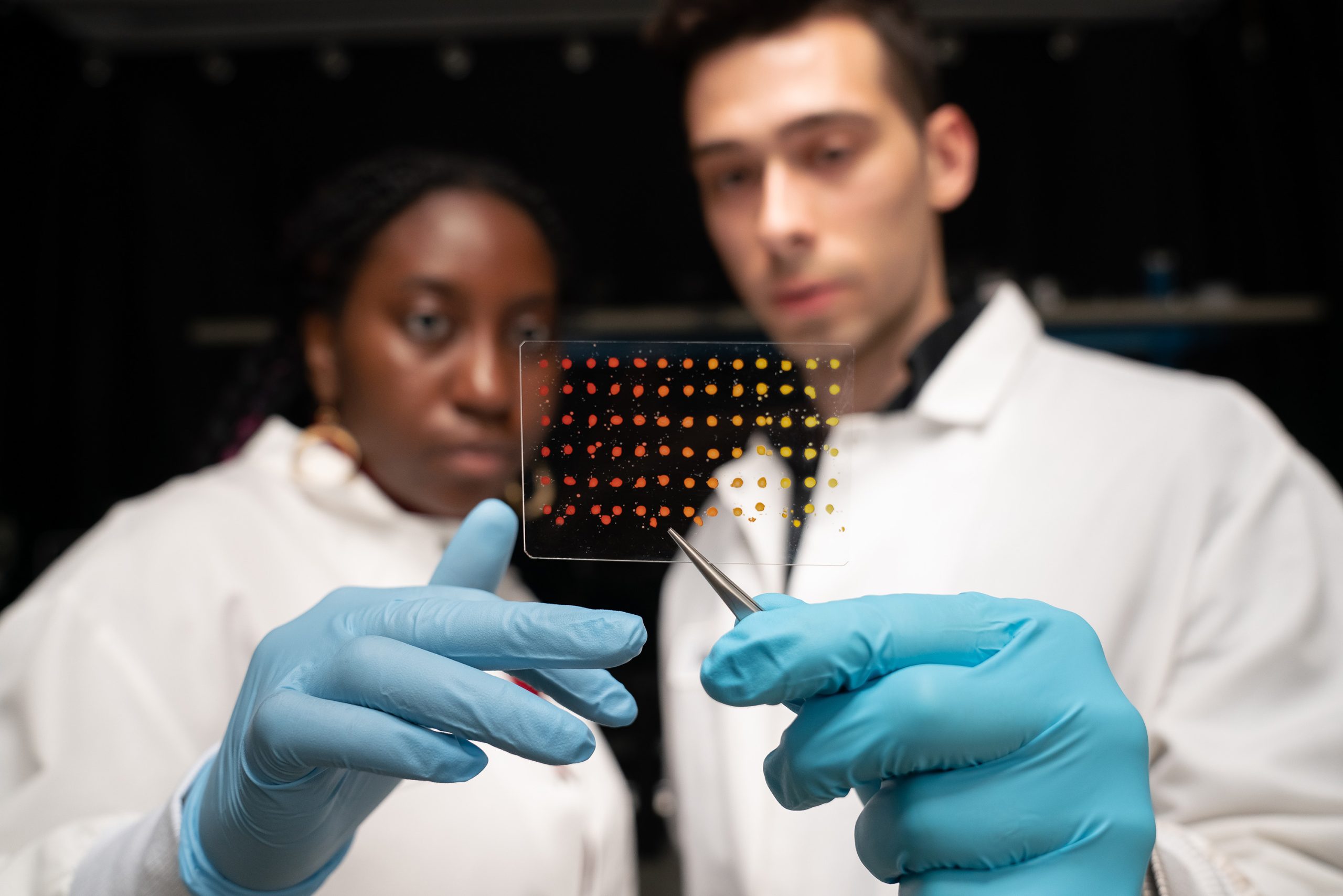
The researchers applied their algorithms to assess band gap and stability in around 70 printed semiconducting samples, utilizing a robotic printer to create a variety of compositions on a single substrate. The focus was on manipulating perovskite materials, which are promising candidates for solar cells yet notorious for their instability over time.
“Researchers are tirelessly working to fine-tune these compositions, exploring various mixes to enhance perovskites’ stability and performance,” notes Buonassisi.
After creating 70 distinct perovskite compositions, the team employed a hyperspectral camera to scan the slide and applied their band gap algorithm, completing the analysis in approximately six minutes—an endeavor that would traditionally consume several days for a domain expert.
For the stability assessment, the slide was placed in an environmental chamber where conditions like humidity, temperature, and light exposure were altered. Using a standard RGB camera, the team captured images every 30 seconds over two hours, applying the stability algorithm to quantify color changes and ultimately calculate a “stability index” for each sample.
Comparing the results against manual measurements taken by domain experts revealed that their newly developed algorithms achieved impressive results—98.5% accuracy for band gap and 96.9% for stability—while operating 85 times faster.
“We were continuously amazed at the algorithms’ ability to not only accelerate characterization but to deliver precise results,” Siemenn expresses. “We see this technology integrating seamlessly into our automated materials pipeline, allowing us to efficiently discover and evaluate new materials using machine learning, continuous manufacturing, and rapid characterization.”
This research was partially supported by First Solar.
Photo credit & article inspired by: Massachusetts Institute of Technology


